Showing posts with label nanotechnologies. Show all posts

Wednesday, January 3, 2007

Cheaper LEDs from breakthrough in ZnO nanowire research

P-type ZnO Nanowires

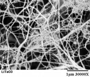
SEM image of p-type ZnO nanowires created by electrical engineering professor Deli Wang at UC San Diego . Note: the blue color was added in photoshop. Credit: Deli Wang/UCSD

Engineers at UC San Diego have synthesized a long-sought semiconducting material that may pave the way for an inexpensive new kind of light emitting diode (LED) that could compete with today's widely used gallium nitride LEDs, according to a new paper in the journal Nano Letters.

To build an LED, you need both positively and negatively charged semiconducting materials; and the engineers synthesized zinc oxide (ZnO) nanoscale cylinders that transport positive charges or "holes" – so-called "p-type ZnO nanowires." They are endowed with a supply of positive charge carrying holes that, for years, have been the missing ingredients that prevented engineers from building LEDs from ZnO nanowires. In contrast, making "n-type" ZnO nanowires that carrier negative charges (electrons) has not been a problem. In an LED, when an electron meets a hole, it falls into a lower energy level and releases energy in the form of a photon of light.
Deli Wang, an electrical and computer engineering professor from UCSD's Jacobs School of Engineering, and colleagues at UCSD and Peking University, report synthesis of high quality p-type zinc oxide nanowires in a paper published online by the journal Nano Letters.
"Zinc oxide nanostructures are incredibly well studied because they are so easy to make. Now that we have p-type zinc oxide nanowires, the opportunities for LEDs and beyond are endless," said Wang.
Wang has filed a provisional patent for p-type ZnO nanowires and his lab at UCSD is currently working on a variety of nanoscale applications.
"Zinc oxide is a very good light emitter. Electrically driven zinc oxide single nanowire lasers could serve as high efficiency nanoscale light sources for optical data storage, imaging, and biological and chemical sensing," said Wang.
To make the p-type ZnO nanowires, the engineers doped ZnO crystals with phosphorus using a simple chemical vapor deposition technique that is less expensive than the metal organic chemical vapor deposition (MOCVD) technique often used to synthesize the building blocks of gallium nitride LEDs. Adding phosphorus atoms to the ZnO crystal structure leads to p-type semiconducting materials through the formation of a defect complex that increases the number of holes relative to the number of free electrons.

"Zinc oxide is wide band gap semiconductor and generating p-type doping impurities that provide free holes is very difficult – particularly in nanowires. Bin Xiang in my group worked day and night for more than a year to accomplish this goal," said Wang.
The starting materials and manufacturing costs for ZnO LEDs are far less expensive than those for gallium nitride LEDs. In the future, Wang expects to cut costs even further by making p-type and n-type ZnO nanowires from solution.
For years, researchers have been making electron-abundant n-type ZnO nanowire crystals from zinc and oxygen. Missing oxygen atoms within the regular ZnO crystal structure create relative overabundances of zinc atoms and give the semiconductors their n-type, conductive properties. The lack of accompanying p-type ZnO nanowires, however, has prevented development of a wide range of ZnO nanodevices.
While high quality p-type ZnO nanowires have not previously been reported, groups have demonstrated p-type conduction in ZnO thin films and made ZnO thin film LEDs. Using ZnO nanowires rather than thin films to make LEDs would be less expensive and could lead to more efficient LEDs, Wang explained.
Having both n- and p-type ZnO nanowires – complementary nanowires – could also be useful in a variety of applications including transistors, spintronics, UV detectors, nanogenerators, and microscopy. In spintronics applications, researchers could use p-type ZnO nanowires to make dilute magnetic semiconductors by doping ZnO with magnetic atoms, such as manganese and cobalt, Wang explained.
Transistors that rely on the semiconducting properties of ZnO are also now on the horizon. "P-type doping in nanowires would make complementary ZnO nanowire transistors possible," said Wang.

(c) www.physorg.com

Saturday, December 23, 2006

NIST laser-based method cleans up grubby nanotubes

Before carbon nanotubes can fulfill their promise as ultrastrong fibers, electrical wires in molecular devices, or hydrogen storage components for fuel cells, better methods are needed for purifying raw nanotube materials. Researchers at the National Institute of Standards and Technology (NIST) and the National Renewable Energy Laboratory (NREL, Golden, Colo.), have taken a step toward this goal by demonstrating a simple method of cleaning nanotubes by zapping them with carefully calibrated laser pulses.

When carbon nanotubes--the cylindrical form of the fullerene family--are synthesized by any of several processes, a significant amount of contaminants such as soot, graphite and other impurities also is formed. Purifying the product is an important issue for commercial application of nanotubes.

Before and after electron microscope images of a pyroelectric detector coated with single-walled nanotubes (SWNTs) visually demonstrate the effect of the laser cleaning process. In addition, the SWNTs look visibly blacker after laser treatment, suggesting less graphitic material and increased porosity. Credit: NIST

In a forthcoming issue of Chemical Physics Letters, the NIST/NREL team describes how pulses from an excimer laser greatly reduce the amount of carbon impurities in a sample of bulk carbon single-walled nanotubes, without destroying tubes. Both visual examination and quantitative measurements of material structure and composition verify that the resulting sample is "cleaner." The exact cleaning process may need to be slightly modified depending on how the nanotubes are made, the authors note. But the general approach is simpler and less costly than conventional "wet chemistry" processes, which can damage the tubes and also require removal of solvents afterwards.

"Controlling and determining tube type is sort of the holy grail right now with carbon nanotubes. Purity is a key variable," says NIST physicist John Lehman, who leads the research. "Over the last 15 years there's been lots of promise, but when you buy some material you realize that a good percentage of it is not quite what you hoped. Anyone who thinks they're going into business with nanotubes will realize that purification is an important--and expensive--step. There is a lot of work to be done."

The new method is believed to work because, if properly tuned, the laser light transfers energy to the vibrations and rotations in carbon molecules in both the nanotubes and contaminants. The nanotubes, however, are more stable, so most of the energy is transferred to the impurities, which then react readily with oxygen or ozone in the surrounding air and are eliminated. Success was measured by examining the energy profiles of the light scattered by the bulk nanotube sample after exposure to different excimer laser conditions. Each form of carbon produces a different signature.

Changes in the light energy as the sample was exposed to higher laser power indicated a reduction in impurities. Before-and-after electron micrographs visually confirmed the initial presence of impurities (i.e., material that did not appear rope-like) as well as a darkening of the nanotubes post-treatment, suggesting less soot and increased porosity.

The researchers developed the new method while looking for quantitative methods for evaluating laser damage to nanotube coatings for next-generation NIST standards for optical power measurements (see http://www.physorg.com/news2821.html). The responsivity of a prototype NIST standard increased 5 percent after the nanotube coating was cleaned.

Citation: K.E. Hurst, A.C. Dillon, D.A. Keenan and J.H. Lehman. Cleaning of carbon nanotubes near the [pi]-plasmon resonance. Chemical Physics Letters, In Press, Corrected Proof. Available online 15 November 2006.

(c) www.physorg.com

Wednesday, December 6, 2006

Danger? Nanotube-Infested Waters Created in the Lab


Carbon nanomaterials can mix in water despite being hydrophobic, raising the possibility of a spreading spill in the future.Carbon Nanotubes

Carbon nanotubes--and their spherical cousins known as buckyballs--are proving to have myriad uses, finding employ in improved solar cells, electronics and medical probes. But the production volume of the tricky nanomaterials remains nanoscale when compared with the production volume of other industrial components. Nevertheless, environmental engineers have begun investigating how such materials might interact with natural environments if accidentally released and have discovered that at least some of the hydrophobic (water fearing) materials persist quite readily in natural waters.
Jae-Hong Kim of the Georgia Institute of Technology and his colleagues investigated how so-called multiwalled carbon nanotubes--layered, straws-within-straws of carbon atoms--interacted with natural water, in this case samples taken from the nearby Suwannee River. To their surprise, the carbon nanomaterial did not clump together as it tried to avoid water molecules, rather it interacted with the negatively charged natural organic matter in the river water. This organic matter seemed to shield the nanotubes and allow them to disperse throughout the water after an hour of mixing, instead of clumping and settling. "At the beginning, the solution is very black and, over time, it becomes grayish," Kim says. "What is interesting is that it is still grayish after a month." In other words, the nanotubes do not settle even after this time period.
This monthlong suspension means that Suwannee River water was actually better at promoting the dispersal of carbon nanotubes than chemical surfactants, which can maintain nanotubes in solution for roughly four days, according to the paper presenting the finding published online in Environmental Science and Technology. Similar studies with buckyballs--stable balls of 60 carbon atoms, also known as C60--had required copious organic solvents in order to maintain suspensions.

Because of the presence of such solvents, toxicity tests on C60 have been open to question as to whether the buckyballs or the solvents caused the damaging effects. Environmental engineers Volodymyr Tarabara and Syed Hashsham of Michigan State University and their colleagues tested the toxic effects of such buckyballs in water--without solvents--on lymphocytes, human immune cells. The researchers created solutions of C60 and water using ethanol at levels previously proven to have no toxic impact and using weeks worth of magnetically powered stirring.
At concentrations as low as 2.2 micrograms per liter, the clumps of C60 damaged the DNA of the immune cells, according to microscopic analysis presented in the December 1 issue of Environmental Science and Technology. The exact mechanism by which C60causes the DNA damage remains unclear, particularly because imaging could not detect the smallest of the buckyball clumps, but its DNA damaging effect was dose dependent. "We are not sure if very very small particles exist, one or two nanometers big," Tarabara says. "They may be very important as far as cellular damage."
Regardless, such nanopollution is unlikely to occur anytime soon: "The fact of the matter is that it takes weeks of mixing to generate appreciable concentrations in the size range where the particles are small enough not to settle," Tarabara notes. "It's not something that we can expect to be out there loose." But the environmental engineers argue that such research should be carried out before any widespread adoption of the new carbon nanomaterials takes place, especially because they seem to have a few surprises in store. "One thing is definite," Kim says, "these materials were not traditionally considered an aqueous-based contaminant." He adds: "I am saying, 'Well, it seems possible.'" --David Biello

[source: www.sciam.com]

Tag Cloud